


News


 电商部
电商部  2025-10-29 16:30:47
 What are the impacts of the main control chip of solid-state drives on performance?
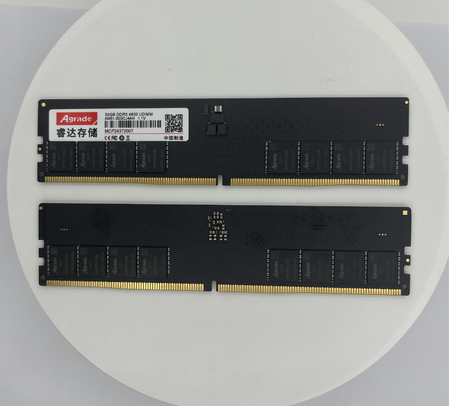
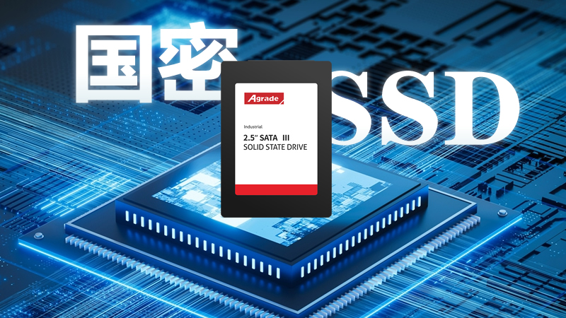
Solid state drives (SSDs) are composed of main control chips, flash memory chips, cache chips (some SSDs have them), and other components. The main control chip is the "brain" of the SSD, which has a comprehensive and critical impact on its performance. The following provides a detailed introduction from multiple aspects:
Data read and write speed
Flash memory management efficiency: The main control chip is responsible for managing the read and write operations of the flash memory chip. An efficient main control chip can accurately and quickly schedule flash memory particles, reducing data read and write latency. For example, the main control chip using advanced algorithms can optimize the storage layout of data in flash memory, enabling read and write instructions to be executed more quickly. Taking the Samsung 870EVO series main control chip as an example, it has excellent flash memory management capabilities, with sequential read speeds easily reaching 560MB/s and sequential write speeds reaching 530MB/s. This is largely due to the efficient allocation of flash memory resources by the main control.
Interface protocol support: The interface protocol supported by the main control chip determines the theoretical bandwidth limit for data transmission. Common interface protocols include SATA, PCIe, etc., among which PCIe interface protocols are divided into different versions (such as PCIe 3.0, PCIe 4.0, etc.). The main control chip that supports higher versions of PCIe protocol can provide higher bandwidth. For example, the main control chip launched by Huirong Technology that supports PCIe 4.0 protocol, combined with NVMe protocol, can make the sequential read speed of SSD exceed 7000MB/s, and the sequential write speed can also exceed 6000MB/s, significantly improving the performance of SSD compared to traditional SATA interface.
Data storage reliability
Error verification and repair: During data storage, data errors may occur due to the physical characteristics of flash memory chips and other reasons. The main control chip integrates error checking and repair mechanisms, such as the common BCH (Bose Chaudhuri Hocquenghem) error correction code technology. High performance main control chips can quickly detect data errors and repair them in a timely manner, ensuring the accuracy and completeness of data. Some high-end SSD control chips from Intel have powerful BCH error correction capabilities, which can correct larger byte errors and greatly improve the reliability of data storage.
Wear and tear balance: Flash memory chips have a limited erase and write life, and uneven erase and write cycles of different storage units can lead to premature damage of some units, thereby affecting the overall lifespan of SSDs. The main control chip uses wear leveling algorithm to evenly distribute data across various flash memory units, avoiding overuse of certain units. For example, the main control chip of Qunlian Electronics adopts advanced dynamic and static wear balance technology, which can effectively extend the service life of SSDs and maintain stable performance even after long-term use.
cache management
Cache scheduling: Some SSDs are equipped with cache chips, and the main control chip is responsible for managing the use of cache. It can intelligently determine which data needs to be prioritized for storage in the cache and which data can be cleared from the cache to improve cache hit rates. When users read data, the main control chip can quickly determine whether the data is in the cache. If it is, it can be directly read from the cache, greatly speeding up the reading speed. For example, some SSD control chips from Micron have significantly improved data read and write performance through efficient cache scheduling mechanisms and large capacity DRAM cache.
Cache type support: The main control chip's support for different types of caches can also affect performance. In addition to traditional DRAM caching, some main control chips also support SLC caching technology. SLC cache uses TLC or QLC flash memory to simulate the working mode of SLC flash memory. The main control chip can flexibly store commonly used data in the SLC cache to improve read and write speed. For example, the TiPlus 7100 SSD, with its main control chip and SLC cache technology, can achieve high read and write performance even without independent DRAM cache.
Compatibility and stability
Hardware compatibility: The main control chip needs to be well compatible with hardware devices such as flash memory chips, cache chips, and computer motherboards. High quality control chips can adapt to flash memory chips of different brands and specifications, ensuring stable data transmission. For example, Marvel's main control chip has been adopted by multiple SSD manufacturers due to its excellent compatibility, which can stably match flash memory chips produced by different manufacturers, providing users with a reliable user experience.
Firmware update support: The firmware of the main control chip determines its functionality and performance. Manufacturers can optimize the algorithm of the main control chip, solve compatibility issues, and improve performance by updating firmware. For example, Samsung regularly releases firmware updates for its SSD controller chips, and users can find that the performance of SSDs has been further optimized and stability has been improved after the updates.

-
Products
Advantages
-
Solutions
-
News
About us
-
Contact us
Tel:+86 19926658803
Whatsapp:+86 19926658803
lianle1210@163.com
Address: 30CF, Caihong Building, Caihong Road, Futian District, Shenzhen City, Guangdong Province, China


Friendly Links:
