
News
 电商部
电商部  2026-01-04 16:05:57
 Prospects of Domestic HBM Memory Technology: How TSV Stacking Ushers in the Era of High Bandwidth
Prospects of Domestic HBM Memory Technology: How TSV Stacking Ushers in the Era of High Bandwidth
HBM (High-Bandwidth Memory) is the next-generation memory technology tailored for high-end scenarios such as AI and supercomputing. Utilizing a 3D stacking architecture, it enables ultra-high bandwidth transmission and has become a focal point of competition in the global storage industry. Changxin Memory Technology has announced the initiation of HBM3 sample research and development, intending to adopt TSV (Through-Silicon Via) stacking technology. This marks the official foray of domestic memory modules into the high-end HBM domain. Understanding the technological advancements of domestic HBM is crucial for grasping the future trajectory of the domestic storage industry.
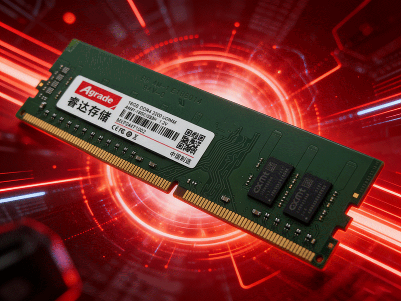
The core advantage of HBM lies in the ultra-high bandwidth brought by its 3D stacked architecture. Traditional memory employs planar packaging, resulting in longer data transmission paths and limited bandwidth. In contrast, HBM utilizes TSV technology to vertically stack multiple DRAM chips, shortening the data transmission path to the nanometer scale. Additionally, it adopts a wide-bit interface design, significantly enhancing bandwidth. According to the JEDEC standard, a single HBM3 can achieve a bandwidth of up to 819GB/s, and when stacked with four chips, the total bandwidth can exceed 3200GB/s, far surpassing traditional DDR5 memory and perfectly meeting scenarios with extremely high bandwidth requirements, such as AI model training.
TSV technology serves as the core backbone for HBM to achieve 3D stacking. By etching tiny conductive vias on silicon wafers, TSV technology facilitates vertical electrical connections between different chip layers, essentially constructing a "three-dimensional transportation network" for chips. Changxin Memory has amassed extensive R&D experience in TSV technology and intends to adopt multi-wafer splicing to achieve higher levels of stacking. Currently, the mainstream international HBM products feature 8-12 stacked layers. Changxin Memory aims to achieve stacking beyond 16 layers, further enhancing storage capacity and bandwidth.
The research and development of domestically produced HBM holds significant strategic importance. Currently, the global HBM market is monopolized by Samsung and SK Hynix, posing security risks to the storage supply chain of high-end devices such as AI accelerators. The imminent delivery of Changxin Memory's HBM3 samples will break the international monopoly and lay a solid storage foundation for the domestic computing power ecosystem. It is anticipated that domestically produced HBM will achieve mass production by 2027, initially supplying domestic data centers and AI enterprises, and subsequently expanding to the global market. As HBM technology matures, domestically produced memory modules will achieve comprehensive breakthroughs in the high-end storage field.

